Beat Frequency Oscillator
The beat frequency oscillator (bfo) is necessary when you want to receive cw signals. Cw signals are not modulated with an audio component, you remember, so we must provide one. The action of the rf amplifier, mixer, local oscillator, and IF amplifier is the same for both cw and AM; but the cw signal reaches the detector as a single frequency signal with no sideband components.
To produce an af output, you must heterodyne (beat) any cw signal with an rf signal of the proper frequency. This separate signal is obtained from an oscillator known as a beat frequency oscillator.
The picture below is a block diagram of a superheterodyne receiver capable of receiving and demodulating a cw signal. The bfo heterodynes at the detector and produces an af output. The detector (second detector) is used primarily because the mixer (first detector) is normally used as the source of agc.

Placement of the beat frequency oscillator.
If the intermediate frequency is 455 kilohertz and the beat frequency oscillator is tuned to 456 kilohertz or 454 kilohertz, the difference frequency of 1 kilohertz is heard in the output. Generally, you will tune the bfo from the front panel of a receiver. When you vary the bfo control, you are varying the output frequency of the bfo and will hear changes in the tone of the output audio signal.
Squelch
The sensitivity of a receiver is maximum when no signal is being received. This condition occurs, for example, when a receiver is being tuned between stations. At this time background noise is picked up by the antenna, and you will hear noise greatly amplified. This noise is highly annoying and occurs because receiver gain is maximum without a signal. You can often overcome this problem by using a circuit called a SQUELCH, NOISE SILENCER, NOISE SUPPRESSOR, or NOISE LIMITER.
All of these noise type circuits just clip the peaks of the noise spikes. Squelch will actually eliminate noise. The picture below is a typical circuit of this type. The circuit cuts off receiver output when no input signal is being received. It accomplishes this by blocking either the detector or audio amplifier when no signal is present. Let’s take a look at the theory involved in this process.

Squelch circuit.
The squelch diode CR1 connects the output of the first af stage to the input of the second. Amplifier Q1 serves as the control transistor for the circuit. The anode and cathode voltages of CR1 are normally biased positive with respect to ground.
With no input signal, R9 is adjusted until Q1 draws enough collector current to reduce its collector voltage and the anode voltage of CR1 to a value below the voltage on the cathode of CR1. At this point the anode voltage of the squelch diode is negative with respect to its cathode, and conduction ceases. Audio output is now reduced to zero and the receiver is silent.
The base of Q1 is connected to the automatic volume control (avc) line. Anytime a signal enters the receiver, a negative avc voltage is applied to the base of Q1. This reduces the collector current and increases the collector voltage, which in turn increases the anode voltage of CR1 until the anode becomes positive with respect to the cathode. Once again diode CR1 will conduct, and the signal will be passed to the second af amplifier. Diode CR1 is effectively a switch controlled by the avc voltage.
(back)
(top)
(next)
(return to communications page)


Download the NEETS for your own library.
If you would like to download the entire set or just one module for a small fee, click on the highlighted NEETS link.
Become a loyal member to our site. It's free!
Site Search

Tweet


Translate your page
If English is not your first language you can Translate the text on this page to any one of the languages found in the drop down menu. Select your language from the list for an instant translation.
Looking for something unique for your project? Choose from the drop down menu for quick access to the item you seek.
Related Pages
Docircuits interactive circuit simulator
Become an Electronics Technician

Convert most anything with this utility
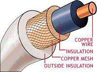
Find your wire and cable here!
Sponsored Sites

Around The World!
Click on the Clustrmaps to see where other people are learning about electronics.

Sponsors help support this site. You can help too!
If you like what you have seen please pay it forward. Donations are welcome.