Common Base Transistor
The common base configuration (CB) shown in the illustration below, view B is mainly used for impedance matching, since it has a low input resistance (30 ohms-160 ohms) and a high output resistance (250 kilohms-550 kilohms). However, two factors limit its usefulness in some circuit applications: (1) its low input resistance and (2) its current gain of less than 1. Since the CB configuration will give voltage amplification, there are some additional applications, which require both a low-input resistance and voltage amplification, that could use a circuit configuration of this type; for example, some microphone amplifiers.
In the common base configuration, the input signal is applied to the emitter, the output is taken from the collector, and the base is the element common to both input and output. Since the input is applied to the emitter, it causes the emitter-base junction to react in the same manner as it did in the common-emitter circuit. For example, an input that aids the bias will increase transistor current, and one that opposes the bias will decrease transistor current.
Unlike the common-emitter circuit, the input and output signals in the common base circuit are in phase. To illustrate this point, assume the input to the PNP version of the common base circuit in the figure above, view B is positive. The signal adds to the forward bias, since it is applied to the emitter, causing the collector current to increase. This increase in Ic results in a greater voltage drop across the load resistor RL (not shown), thus lowering the collector voltage V C. The collector voltage, in becoming less negative, is swinging in a positive direction, and is therefore in phase with the incoming positive signal.
The current gain in the common-base circuit is calculated in a method similar to that of the common emitter except that the input current is I E not IB and the term ALPHA (a) is used in place of beta for gain. Alpha is the relationship of collector current (output current) to emitter current (input current). Alpha is calculated using the formula:

Transistor configurations.
For example, if the input current (IE) in a common base changes from 1 mA to 3 mA and the output current (I C) changes from 1 mA to 2.8 mA, the current gain (a) will be 0.90 or:

This is a current gain of less than 1.
Since part of the emitter current flows into the base and does not appear as collector current, collector current will always be less than the emitter current that causes it. (Remember, IE = IB + IC) Therefore, ALPHA is ALWAYS LESS THAN ONE FOR A COMMON-BASE CONFIGURATION.
Another term for "a" is hf. These terms (and hf) are equivalent and may be used interchangeably. The meaning for the term hf is derived in the same manner as the term hfe mentioned earlier, except that the last letter "e" has been replaced with "b" to stand for common- base configuration.
Many transistor manuals and data sheets only list transistor current gain characteristics in terms of b or hfe. To find alpha (a) when given beta (b), use the following formula to convert b to a for use with the common-base configuration:

To calculate the other gains (voltage and power) in the common-base
configuration when the current gain (a) is known, follow the procedures
described earlier under the common-emitter section.
(back) (top) (next) (return to transistor page)


Download the NEETS for your own library.
If you would like to download the entire set or just one module for a small fee, click on the highlighted NEETS link.
Become a loyal member to our site. It's free!
Site Search

Tweet


Translate your page
If English is not your first language you can Translate the text on this page to any one of the languages found in the drop down menu. Select your language from the list for an instant translation.
Looking for something unique for your project? Choose from the drop down menu for quick access to the item you seek.
Related Pages

Docircuits interactive circuit simulator
Become an Electronics Technician

Convert most anything with this utility
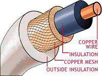
Find your wire and cable here!
Sponsored Sites


Around The World!
Click on the Clustrmaps to see where other people are learning about electronics.
