PN Barrier Junction
PN Barrier Junction of a Semiconductor Diode
Although the N-type material has an excess of free electrons, it is still electrically neutral. This is because the donor atoms in the N material were left with positive charges after free electrons became available by covalent bonding (the protons outnumbered the electrons). Therefore, for every free electron in the N material, there is a corresponding positively charged atom to balance it.
The end result is that the N material has an overall charge of zero. By the same reasoning, the P-type material is also electrically neutral because the excess of holes in this material is exactly balanced by the number of electrons.
Keep in mind that the holes and electrons are still free to move in the material because they are only loosely bound to their parent atoms. It would seem that if we joined the N and P materials together by one of the processes mentioned earlier, all the holes and electrons would pair up.
On the contrary, this does not happen. Instead the electrons in the N material diffuse (move or spread out) across the junction into the P material and fill some of the holes. At the same time, the holes in the P material diffuse across the junction into the N material and are filled by N material electrons.
This process, called JUNCTION RECOMBINATION, reduces the number of free electrons and holes in the vicinity of the junction. Because there is a depletion, or lack of free electrons and holes in this area, it is known as the DEPLETION REGION.
The loss of an electron from the N-type material created a positive ion in the N material, while the loss of a hole from the P material created a negative ion in that material. These ions are fixed in place in the crystal lattice structure and cannot move. Thus, they make up a layer of fixed charges on the two sides of the junction as shown in the illustration below.

PN barrier junction formation in a semiconductor diode.
On the N side of the junction, there is a layer of positively charged ions; on the P side of the junction, there is a layer of negatively charged ions. An electrostatic field, represented by a small battery in the illustration, is established across the junction between the oppositely charged ions.
The diffusion of electrons and holes across the junction will continue until the magnitude of the electrostatic field is increased to the point where the electrons and holes no longer have enough energy to overcome it, and are repelled by the negative and positive ions respectively.
At this point equilibrium is established and, for all practical purposes, the movement of carriers across the junction ceases. For this reason, the electrostatic field created by the positive and negative ions in the depletion region is called a barrier.
The action just described occurs almost
instantly when the junction is formed. Only the carriers in the
immediate vicinity of the junction are affected. The carriers throughout
the remainder of the N and P material are relatively undisturbed and
remain in a balanced condition.
(back) (top) (return to diodes page)
Your first paragraph ...


Download the NEETS for your own library.
If you would like to download the entire set or just one module for a small fee, click on the highlighted NEETS link.
Become a loyal member to our site. It's free!
Site Search

Tweet


Translate your page
If English is not your first language you can Translate the text on this page to any one of the languages found in the drop down menu. Select your language from the list for an instant translation.
Looking for something unique for your project? Choose from the drop down menu for quick access to the item you seek.
Related Pages
Docircuits interactive circuit simulator
Become an Electronics Technician

Convert most anything with this utility
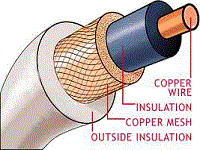
Find your wire and cable here!
Sponsored Sites

Around The World!
Click on the Clustrmaps to see where other people are learning about electronics.

Sponsors help support this site. You can help too!
If you like what you have seen please pay it forward. Donations are welcome.