Doping Process
Doping Process
The semiconductor (diode) mentioned in the basic electronics tutorial on covalent bonding and conduction is essentially neutral.
It contains no free electrons in its conduction bands. Even with the application of thermal energy, only a few covalent bonds are broken, yielding a relatively small current flow.
A much more efficient method of increasing
current flow insemiconductors is by adding very small amounts of
selected additives to them, generally no more than a few parts per
million. These additives are called impurities and the process of adding
them to crystals is referred to as the doping process.
The purpose of semiconductor doping is to increase the number of free charges that can be moved by an external applied voltage.
When an impurity increases the number of free electrons, the doped semiconductor is NEGATIVE or N TYPE, and the impurity that is added is known as an N-type impurity. However, an impurity that reduces the number of free electrons, causing moreholes, creates a POSITIVE or P-TYPE semiconductor, and the impurity that was added to it is known as a P-type impurity.
Semiconductors which are doped in this manner — either with N- or P-type impurities — are referred to as EXTRINSIC semiconductors.
P and N type semiconductors will be presented in detail in following tutorials.
(back)
(top)
(next)
(return to diodes page)


Download the NEETS for your own library.
If you would like to download the entire set or just one module for a small fee, click on the highlighted NEETS link.
Become a loyal member to our site. It's free!
Site Search

Tweet


Translate your page
If English is not your first language you can Translate the text on this page to any one of the languages found in the drop down menu. Select your language from the list for an instant translation.
Looking for something unique for your project? Choose from the drop down menu for quick access to the item you seek.
Related Pages
Docircuits interactive circuit simulator
Become an Electronics Technician

Convert most anything with this utility
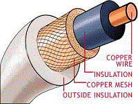
Find your wire and cable here!
Sponsored Sites

Around The World!
Click on the Clustrmaps to see where other people are learning about electronics.

Sponsors help support this site. You can help too!
If you like what you have seen please pay it forward. Donations are welcome.